Magnifying into microscopes
Do you feel like digging deeper into the things we see everyday? Do you want to see the world at a microscopic level? Then here's your guide to MICRO-scopes!
|
|
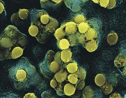
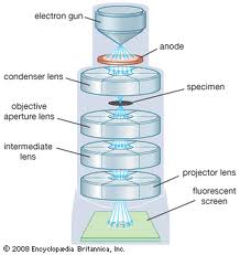
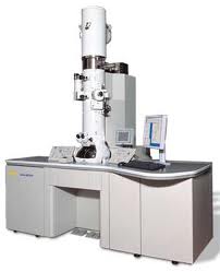
I certainly have to comment that the microscope is one of the most invaluable tools in scientific research to me. Without it, I doubt any of us would have the tools to build microprocessors, observe the millions of cells all over the Earth, or study the details of elements, mixtures and compounds. Advances in microscopy have contributed to major discoveries in the many fields of science. It has allowed, and continues to allow, us to study virtually everything at the minute level. Today, many student laboratories high schools, colleges and universities are equipped with light microscopes for observing different objects and processes to aid us in learning. Electron microscopes, those that give extreme amounts of magnification and resolution, are being used by scientists all over the world.
|
|
|
It all started during 1950, when Dutch lens grinders called Hans and Zacharias Janssen placed two lenses in a tube, forming the first ever microscope. In the 18th century, many advancements occurred, and many scientists devised ways to improve the functionality and usability of the microscope. Microscopes have become an undeniable partner of most of the lives of scientists in the world today!

Let me elaborate more on a particular kind of microscope, the Scanning Tunnelling Microscope (STM)
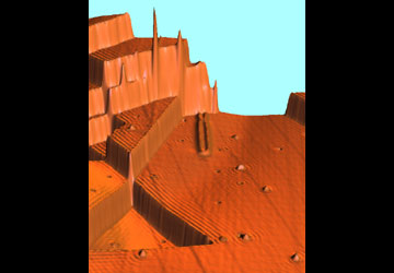
Simply put, it is just another form of electron microscope that shows 3-D images of a sample. Nobel Laureates Heinrich Rohrer and Gerd Binnig made it. It works by allowing a fine conducting probe to be held very close to the sample and an electrical signal is produced. The stylus which scans the sample is only 1 atom thick, and it scans the sample at the same precision as its size! This scans even the smallest details of the sample.
The piezoelectric effect, created by squeezing the sides of certain crystals like quartz, has been used for it. Therefore, by applying a voltage across a piezoelectric crystal, it will elongate or compress. Lead Zirconium Titanate is the piezoelectric material most commonly used in the tip of a STM. Finally, a computer-generated contour map of the surface is produced.
Why do we need to view things at such a small level? This is most applicable to semiconductor physics and microelectronics. Chemistry also requires this, because catalysis needs the understanding of surface reactions. In biology, the STM has been used in the study of DNA molecules.
For fun, have a look at this interesting simulation! click below:
(From nobelprize.org)
